PCB panelization is a technique of manufacturing a collection of PCBs together on a single larger panel which can foster the easy movements of PCBs through an assembly line. Each board in the panel can be of the same or a different design. After production, the panel can easily be separated into individual boards. Panelization is commonly used to optimize and increase efficiency in the production of small and odd-shaped PCBs. For PCBs smaller than 50mm x 50mm, panelization is recommended.
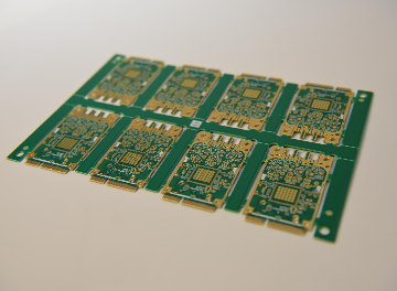
Figure 1: PCB panelization
Depanelization methods
Depanelization is the separation of individual circuit boards from the PCB panel. It can be carried out in different ways:
V-Scoring
V-scoring is a technique that involves cutting a V-shaped groove into a panel to separate the individual boards. The size of the groove is an important parameter, especially its "remained thickness," which is the thickness of the board left between the two inverted V-grooves. The most common residual thickness is recommended to be 1/3 of the thickness of the board.
However, as V-scores must be straight lines on the panel, this method has some restrictions. For example, panels with irregular shapes or complex cutouts may not be suitable for V-Scoring. Also, it is not suggested to use the V-Scoring method where components are hanging over the edge as the components could be damaged during the separation process. In such cases, alternative separation methods, such as tab-routing may be more appropriate.

Figure 2: V-Scoring
Tab routing
In this method, tabs are created along the edges of each board. Tab routing panelization is a flexible method that can accommodate irregularly shaped PCBs and components that extend beyond the edge of the board. To use tab routing, the tabs must be designed to be strong enough to hold the board in place during assembly and testing, but also thin enough to be easily cut or broken after assembly.
In some cases, tabs are routed with additional perforations or stamp holes. The perforations in the tabs make it easier to separate the individual PCBs from the panel. Additionally, by breaking off the tabs along the perforations, the stress is distributed evenly across the edge of the PCB, reducing the risk of damage or deformation.
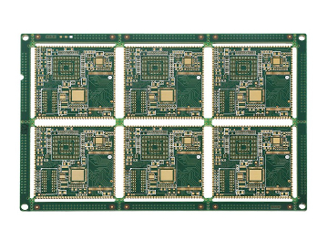
Figure 3: Tab routing
In addition to tab routing, breakaway rails can also be included in the panelization design. Breakaway rails are thin strips of material that are added to the edges of the panel to provide extra support during the manufacturing process. The width of the breakaway rail is generally about 5-8mm. The rails can be easily broken off after the boards are assembled and tested, leaving clean and smooth edges on the individual PCBs.
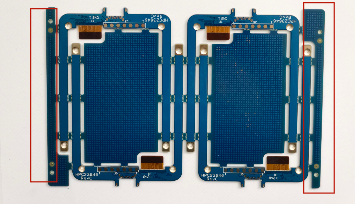
Figure 4: Breakaway rails


