What is PCB Back Drilling?
Back drilling is a technique used to remove via stubs from the inner layers of a multilayer PCB. Via stubs are non-functional portions of plated through-hole or via barrels which can cause unwanted reflections, leading to signal distortion and reduced performance. By eliminating via stubs, back drilling ensures consistent impedance alignment throughout the signal path, minimizing signal reflections and ultimately improving signal quality. If your design contains high-speed communication systems or sensitive analog circuits, back drilling is a good technique to meet your performance requirements.
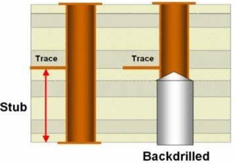
Figure1: PCB Back Drilling
To better understand the use of back drilling, let's consider a simple example. Suppose you design a 10-layer PCB with high-speed signals running between layers 3 to 7. Typically, the via is drilled through all the layers of the board, including layers 8 to 10, where the signal is not required to continue. In such a design, back drilling is performed to remove the via stubs between layers 8 to 10.
How Back Drilling Works?
Back drilling process involves using a CNC machine to drill out the via stubs from the opposite side of the board. The diameter of the back drilled hole should be slightly larger than the diameter of the via, typically around 4-6 mils larger, depending on the via size and board thickness. This ensures that the hole removes the via stub, but does not damage the surrounding copper or dielectric layers.
Factors that Influence the Effectiveness of Back Drilling
Before deciding to use back drilling in your PCB design, there are several factors to consider that can affect its effectiveness.
Board material and thickness:The effectiveness of the back drilling process can be influenced by the material and thickness of the PCB. For example, FR-4 material is commonly used in PCBs and is relatively easy to drill. However, other materials such as ceramic or metal-core boards may require different drill bits and drilling parameters due to their hardness or thermal conductivity.
Via size and spacing:The size and spacing of the vias can also affect the effectiveness of the back drilling process. Smaller vias may require more precise drilling, while larger vias may require larger drill bits or multiple passes.
Trace and plane clearance:Also, it's important to consider the clearance between the drill bit and surrounding features, such as trace and plane layers. In some cases, insufficient clearance can cause the drill bit to accidentally drill through the plane or trace layer, damaging the board.
At PCBWay, you can fill out the details in the blank of "Other Special request" if you need PCB back drilling service.